
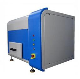
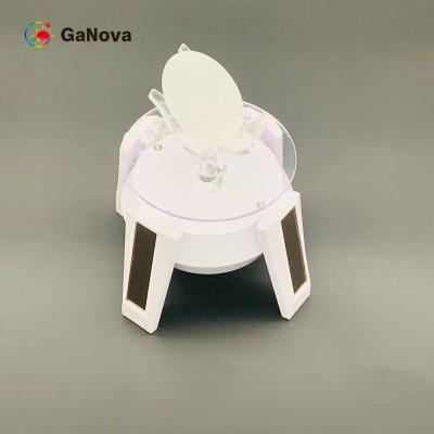
RTP-SA-8 Aufheizungssystem für schnelle thermische Verarbeitung
Preis: Negotiable
MOQ: Negotiable
Lieferzeit: 3 month
Marke: Ganova
Markieren:Boost Production Rapid Thermal Processing, Rapid Thermal Processing Annealing System
1.Basic configuration of equipment system 1.1outline The Rapid Thermal Processing is a vertical semi-automatic 8-inch wafer rapid annealing furnace, which uses two layers of infrared halogen lamps as heat sources for heating. The internal quartz cavity is insulated and insulated, and the outer shell... Mehr sehen
Kontaktieren Sie mich jetzt
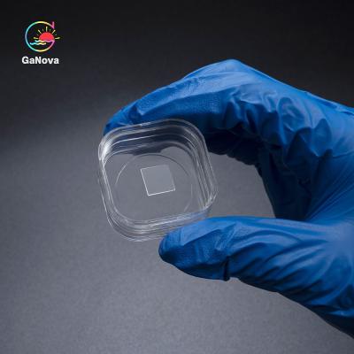
150mm schnelles thermisches Vergütungssystem mit drei Satz-Prozessgasen
Preis: Negotiable
MOQ: 1
Lieferzeit: 8-10week days
Marke: GaNova
Markieren:150mm Rapid Thermal Annealing System, desktop rapid thermal processing equipment, Wafer Rapid Thermal Annealing System
RTP-150RL Rapid Thermal Annealing System with Three Sets Process Gases RTP-150RL: Is in the protection atmosphere of the desktop manual rapid annealing system, with infrared visible light heating single piece Wafer or sample, short process time, high temperature control precision, suitable for 2-6 i... Mehr sehen
Kontaktieren Sie mich jetzt

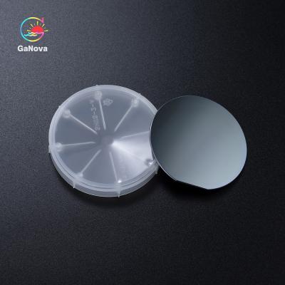
JDCD05-001-003 10*10mm2*0.3mm elektronischer Grad einzelner Crystal Diamond, N Content<100ppb, Wärmeleitfähigkeit XRD<0.015º
Preis: Negotiable
MOQ: Negotiable
Lieferzeit: 3-4 week days
Marke: GaNova
Markieren:Electronic Grade Single Crystal Diamond, 10*10mm2*0.3mm Single Crystal Diamond
10*10mm2*0.3mm einzelner Kristalldiamant elektronischen Grades, Stickstoffgehalt<100ppb>
ÜberblickEinzel-Kristalldiamantoblaten ermöglichen kritischen Fortschritten in beiden die Rf-Energietechnologie, die für Kommunikationen 5G und Satelliten eingesetzt wird; sowie in der Leistungselektr... Mehr sehen
Kontaktieren Sie mich jetzt
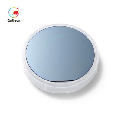
JDCD05-001-006 10*10mm2*0.5mm elektronischer Grad einzelner Crystal Diamond, N Content<100ppb, Wärmeleitfähigkeit XRD<0.015º
Preis: Negotiable
MOQ: Negotiable
Lieferzeit: 3-4 week days
Marke: GaNova
Markieren:10*10mm2*0.5mm Single Crystal Diamond
JDCD05-001-006 10*10mm2*0.5mm einzelner Kristalldiamant elektronischen Grades, Stickstoffgehalt<100ppb>
Überblick
Cvd-Diamant ist lang als das entscheidende Material in einer großen Vielfalt von den Anwendungen wegen seiner extremen Qualitäten erkannt worden.
Für Diamant CVD spielt ... Mehr sehen
Kontaktieren Sie mich jetzt
4 Zoll P-Typ Mg-dotiertes GaN auf Saphir-Wafer SSP-Widerstand ~10 Ω cm LED-Laser-PIN-Epitaxie-Wafer
Preis: Negotiable
MOQ: Negotiable
Lieferzeit: 3-4 week days
Marke: GaNova
Markieren:LED Laser PIN Epitaxial Wafer
4 Zoll Mg-dotiertes GaN vom P-Typ auf Saphirwafer SSP-Widerstand ~10 Ω cm LED, Laser, PIN-Epitaxiewafer
Die elektrischen Eigenschaften von p-Typ Mg-dotiertem GaN werden durch temperaturvariable Hall-Effekt-Messungen untersucht.Proben mit einer Reihe von Mg-Dotierungskonzentrationen wurden durch ... Mehr sehen
Kontaktieren Sie mich jetzt
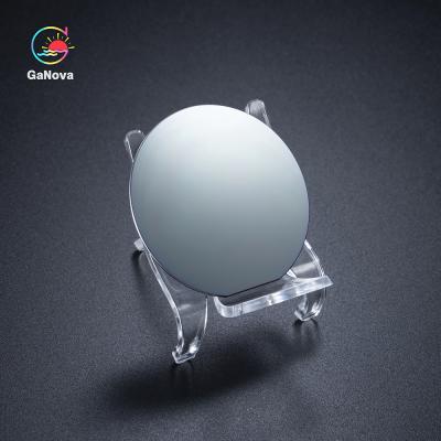
JDCD05-001-005 5 * 5 mm2 * 0,5 mm Einkristall-Diamant in elektronischer Qualität, N-Gehalt < 100 ppb, XRD < 0,015º Wärmeleitfähigkeit
Preis: Negotiable
MOQ: Negotiable
Lieferzeit: 3-4 week days
Marke: GaNova
Markieren:XRD<0.015º Single Crystal Diamond
JDCD05-001-005 5 * 5 mm2 * 0,5 mm Einkristalldiamant in elektronischer Qualität, N-Gehalt < 100 ppb, XRD < 0,015 ° Wärmeleitfähigkeit 1000-2200 für Kühlkörper
Überblick
Die hohe Wärmeleitfähigkeit von Diamant hat ihn für Wärmemanagementanwendungen nützlich gemacht.Sein breiter optischer Ü... Mehr sehen
Kontaktieren Sie mich jetzt
F.E. lackierte GaN Substrates Resistivity > 10 ⁶ Ω·Cm Rf-Geräte
Preis: Negotiable
MOQ: Negotiable
Lieferzeit: 3-4 week days
Marke: GaNova
Markieren:ISO GaN Substrates, gan semiconductor wafer, Fe Doped GaN Substrates
2inch C-face Fe-doped SI-type free-standing GaN single crystal substrate Resistivity > 106 Ω·cm RF devices The achieved breakdown voltage of the Fe-doped GaN epitaxial layer can be as high as 2457 V, which is attributed to the Fe-doped GaN epitaxial layer with higher resistance, which can sustain... Mehr sehen
Kontaktieren Sie mich jetzt
625um flachen dem Saphir zu des Zoll-675um 4 blauen LED GaN Epitaxial Wafer On Sapphire SSP
Preis: Negotiable
MOQ: Negotiable
Lieferzeit: 3-4 week days
Marke: GaNova
Markieren:625um GaN Epitaxial Wafer, SSP gan on sapphire wafers, 675um GaN Epitaxial Wafer
Substrate Thickness 650 ± 25 μm 4 Inch Blue LED GaN Epitaxial Wafer On Sapphire SSP Flat Sapphire 4 inch Blue LED GaN epitaxial wafer on sapphire SSP For example, GaN is the substrate which makes violet (405 nm) laser diodes possible, without use of nonlinear optical frequency-doubling. Its sensitiv... Mehr sehen
Kontaktieren Sie mich jetzt
4 Zoll 4H-SiC Substrat P-Level SI 500.0±25.0μm MPD≤5/cm2 Widerstand≥1E5Ω·cm Für die Mikrowelle
Preis: Negotiable
MOQ: Negotiable
Lieferzeit: 3-4 week days
Marke: GaNova
Markieren:4H-SiC-Substrat auf P-Ebene, Mikrowellen 4H-SiC-Substrat, 4 Zoll 4H-SiC Substrat
JDCD03-002-002 4inch 4H-SiC Substrat P Niveau SI 500.0±25.0μm MPD≤5/cm2 Resistivity≥1E5Ω·cm für Energie- und Mikrowellengeräte
Überblick
Sic wird für die Herstellung von sehr Hochspannungs- und starken Geräten wie Dioden, Leistungstransistoren und Mikrowellengeräten der hohen Leistung ver... Mehr sehen
Kontaktieren Sie mich jetzt
JDCD08-001-006 6inch C-Fläche Sapphire Substrate Wafer
Preis: Negotiable
MOQ: Negotiable
Lieferzeit: Negotiable
Markieren:6inch Sapphire Substrate Wafer
JDCD08-001-006 6inch C-Fläche Sapphire Substrate Wafer
Saphire sind an zweiter Stelle nur zu den Diamanten in der HaltbarkeitDiamant ist das dauerhafteste natürlich vorkommende Element auf Erde und Rängen als 10 aus 10 auf Mohs-Skala von Mineralhärte heraus. Saphire sind auch als 9 aus 10 auf M... Mehr sehen
Kontaktieren Sie mich jetzt

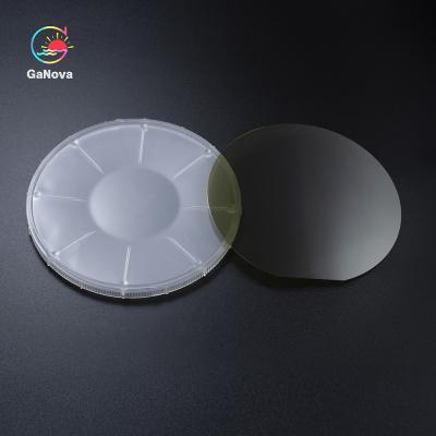
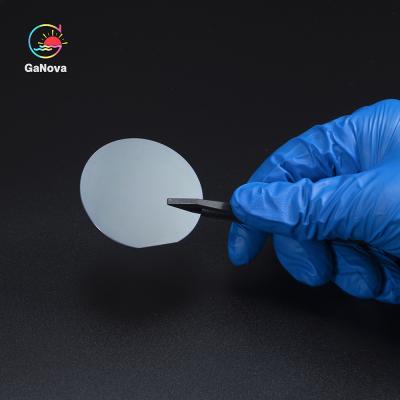
JDCD05-001-007 CVD-Diamantsubstrate
Preis: Negotiable
MOQ: Negotiable
Lieferzeit: 3-4 week days
Marke: GaNova
Markieren:CVD Diamond Substrates, CVD Diamond Substrates 007
JDCD05-001-007 CVD Diamond Substrates
Überblick
Diamant ist ein einzigartiges Material, das häufig die extremen Eigenschaften aufweist, die mit anderen Materialien verglichen werden. Vor entdeckt ungefähr 30 Jahren, hat der Gebrauch des Wasserstoffs in Plasma-erhöhtem chemischem Bedampfen (CVD... Mehr sehen
Kontaktieren Sie mich jetzt

2 Zoll grüne LED GaN auf Siliziumwafer Dimension 520±10nm
Preis: Negotiable
MOQ: Negotiable
Lieferzeit: 3-4 week days
Marke: GaNova
Markieren:2 Zoll GaN auf Siliziumwafer, Grüne LED GaN auf Siliziumwafer, 520nm GaN auf Siliziumwafer
2-Zoll-Grün-LED-GaN auf Siliziumwafer
Überblick
Galliumnitrid (GaN) sorgt für einen innovativen Wandel in der Welt der Leistungselektronik.Seit Jahrzehnten sind MOSFETs auf Siliziumbasis (Metalloxid-Halbleiter-Feldeffekttransistoren) ein fester Bestandteil des modernen Alltags, der dabei hilft,... Mehr sehen
Kontaktieren Sie mich jetzt
JDCD06-001-004 5-Zoll-Siliziumwafer MEMS-Geräte Integrierte Schaltungen dedizierte Substrate für diskrete Geräte
Preis: Negotiable
MOQ: 1
Lieferzeit: 3-4 week days
Marke: GaNova
Markieren:Integrierte Schaltungen Siliziumwafer, Diskrete Geräte Siliziumwafer, 5 Zentimeter große Silikon-Wafer
5-Zoll-Siliziumwafer-MEMS-Geräte, integrierte Schaltkreise, dedizierte Substrate für diskrete Geräte
Überblick
Obwohl Siliziumkristalle metallisch aussehen können, sind sie nicht vollständig Metalle.Aufgrund der „freien Elektronen“, die sich leicht zwischen Atomen bewegen, sind Metalle gute el... Mehr sehen
Kontaktieren Sie mich jetzt

JDCD06-001-005 6-Zoll-Silizium-Wafer-MEMS-Geräte Integrierte Schaltungen dedizierte Substrate für diskrete Geräte
Preis: Negotiable
MOQ: 1
Lieferzeit: 3-4 week days
Marke: GaNova
Markieren:Integrierte Schaltungen Siliziumwafer, Diskrete Geräte Siliziumwafer, Siliziumscheibe
6 Zoll Geräte der Siliziumscheibe MEMS, integrierte Schaltungen, engagierte Substrate für getrennte Geräte
Überblick
Silikon wird gewöhnlich zusammengesetzt mit anderen Elementen gefunden. Silikonelemente sind in der Lage, Atome in den komplexen Vorbereitungen fest und zu binden. Der Überflu... Mehr sehen
Kontaktieren Sie mich jetzt

JDCD06-001-006 8-Zoll-Siliziumwafer MEMS-Geräte Integrierte Schaltungen dedizierte Substrate für diskrete Geräte
Preis: Negotiable
MOQ: 1
Lieferzeit: 3-4 week days
Marke: GaNova
Markieren:Integrierte Schaltungen Siliziumwafer, MEMS-Geräte Siliziumwafer, Diskrete Geräte Siliziumwafer
8-Zoll-Siliziumwafer-MEMS-Geräte, integrierte Schaltkreise, dedizierte Substrate für diskrete Geräte
Überblick
In der Elektronik sind Siliziumwafer (auch bekannt als Substrate) dünne Scheiben aus hochreinem kristallinem Silizium (c-Si), die bei der Herstellung von integrierten Schaltkreisen ve... Mehr sehen
Kontaktieren Sie mich jetzt

JDCD06-001-007 12-Zoll-Siliziumwafer MEMS-Geräte Integrierte Schaltungen dedizierte Substrate für diskrete Geräte
Preis: Negotiable
MOQ: 1
Lieferzeit: 3-4 week days
Marke: GaNova
Markieren:Integrierte Schaltungen Siliziumwafer, Diskrete Geräte Siliziumwafer, 12-Zoll-Silizium-Wafer
12 Zoll Geräte der Siliziumscheibe MEMS, integrierte Schaltungen, engagierte Substrate für getrennte Geräte
ÜberblickEine Siliziumscheibe ist ein Material, das für Herstellungshalbleiter wesentlich ist, die in allen Arten elektronische Geräte gefunden werden, die unsere Leben anreichern. Weni... Mehr sehen
Kontaktieren Sie mich jetzt

JDCD04-001-007 10 x 10 mm2 (010) Sn-dotiertes freistehendes Ga2O3-Einkristall-Substrat Produktqualität Einzelpolierung
Preis: Negotiable
MOQ: Negotiable
Lieferzeit: 3-4 week days
Marke: GaNova
Markieren:Freistehender Ga2O3-Einkristall-Substrat, Produktart Ga2O3 Einkristall Substrat, 10x10mm2 Ga2O3 Einkristall Substrat
10 x 10 mm2 (010) Sn-dotiertes freistehendes Ga2O3-Einkristallsubstrat Produktklasse Einzelpolierung Dicke 0,6 ~ 0,8 mm FWHM < 350 Bogensekunden, Ra ≤ 0,5 nm Widerstand 1,53 E + 18 Ω / cm-3 Optoelektronische Geräte, Isolierschichten aus Halbleitermaterialien und UV-Filter
Während siliziumbasi... Mehr sehen
Kontaktieren Sie mich jetzt
JDCD07-001-001 4-Zoll-SOI-Epitaxialwafer für die MEMS-Verarbeitung
Preis: Negotiable
MOQ: 1
Lieferzeit: 3-4 week days
Marke: GaNova
Markieren:MEMS-Verarbeitung von SOI-Epitaxialwafer, 4-Zoll-SOI-Epitaxialwafer, SOI-Epitaxialwafer
Epitaktischer 4-Zoll-SOI-Wafer für die MEMS-Verarbeitung
Überblick
Obwohl Siliziumkristalle metallisch aussehen können, sind sie nicht vollständig Metalle.Aufgrund der „freien Elektronen“, die sich leicht zwischen Atomen bewegen, sind Metalle gute elektrische Leiter, und Elektrizität ist die B... Mehr sehen
Kontaktieren Sie mich jetzt
JDCD07-001-004 7-Zoll-SOI-Epitaxialwafer für die MEMS-Verarbeitung
Preis: Negotiable
MOQ: 1
Lieferzeit: 3-4 week days
Marke: GaNova
Markieren:7 Zoll SOI Epitaxial Wafer, MEMS-Verarbeitung von SOI-Epitaxialwafer, SOI-Epitaxialwafer
7-Zoll-SOI-Epitaxie-Wafer für die MEMS-Verarbeitung
ÜberblickEin Siliziumwafer ist ein wesentliches Material für die Herstellung von Halbleitern, die in allen Arten von elektronischen Geräten zu finden sind, die unser Leben bereichern.Nur wenige von uns haben die Möglichkeit, im täglichen Leben... Mehr sehen
Kontaktieren Sie mich jetzt
JDCD07-001-002 5-Zoll-SOI-Epitaxialwafer für die MEMS-Verarbeitung
Preis: Negotiable
MOQ: 1
Lieferzeit: 3-4 week days
Marke: GaNova
Markieren:5-Zoll-SOI-Epitaxialwafer, SOI-Epitaxialwafer, MEMS-Verarbeitung von SOI-Epitaxialwafer
5 Zoll Epitaxial- Wafer SOI für MEMS Verarbeitung
Überblick
Siliziumscheiben (Si-Oblate) sind dünne Scheiben des in hohem Grade reinen kristallisierten Silikons. Siliziumscheiben treten als ein Substrat für Mikroelektronische Geräte und sind in errichtenden elektronischen Schaltungen wegen i... Mehr sehen
Kontaktieren Sie mich jetzt