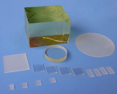
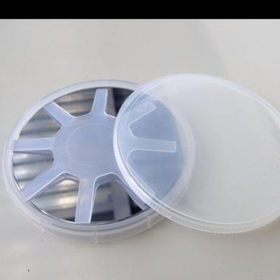
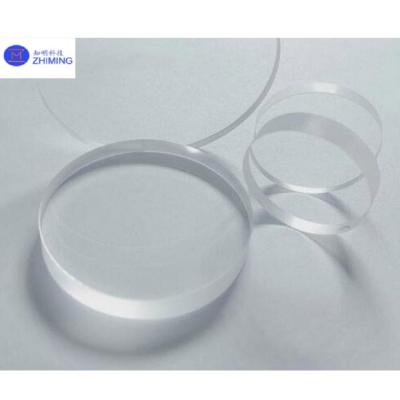
Indium-Phosphid-Oblate
(33)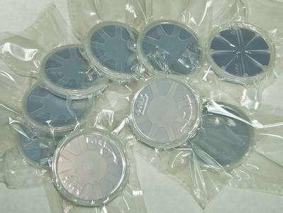
Schwarze Indium-Phosphid-Oblate, Halbleiterwafer für LD-Anwendung
Preis: by case
MOQ: 5pcs
Lieferzeit: 1-4weeks
Marke: zmkj
Markieren:MgO-Substrat, Gap-Oblate
2inch 3inch 4inch InP-Substrate für LD-Anwendung, Halbleiterwafer, InP-Oblate, einzelne Kristallscheibe
InP führen ein
Einzelner Kristall InP
Das tCZ Wachstum (geänderte Czochralski-Methode) wird verwendet, um einen einzelnen Kristall durch ein flüssiges encapsulant... Mehr sehen
➤ Besuch Webseite
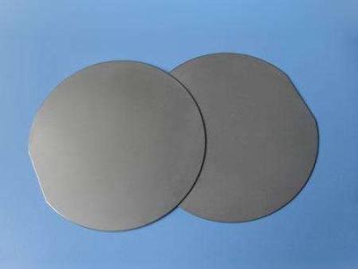
Platten-Indium-Phosphid-Oblaten-ausgezeichnetes Halbleiter-Material GEs optische
Preis: by case
MOQ: 3pcs
Lieferzeit: 1-4weeks
Marke: zmkj
Markieren:MgO-Substrat, Gap-Oblate
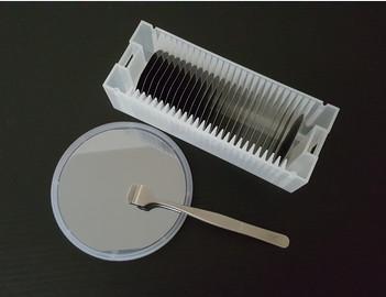
Germanium-einzelne Kristallscheiben, optische Platten GEs
Germaniumsubstrate
Anwendung: Germaniumoblate benutzt in der Produktion des Halbleiterbauelements, optisches Gerät des Infrarotstrahls, sinkendes Material der Solarzelle.
Haupteigentums-Ausdrücke
Produktionsverfa... Mehr sehen
➤ Besuch Webseite
GE-Linsen-Halbleiter-Substrate INP-Indium-Gallium-Phosphid-Oblate
Preis: by case
MOQ: 3pcs
Lieferzeit: 1-4weeks
Marke: zmkj
Markieren:GE-Linse Indium-Phosphid-Oblate, Halbleitersubstrate Indium-Phosphid-Oblate, einzelner Kristall inp GEs
Germanium-einzelne Kristall-GE-Substrate Oblaten 4inch 6inch, kundengebundene optische Linse GEs
Germaniumsubstrate
Anwendung: Germaniumoblate benutzt in der Produktion des Halbleiterbauelements, optisches Gerät des Infrarotstrahls, sinkendes Material der Solarzelle.
Haupteigentums-Ausd... Mehr sehen
➤ Besuch Webseite
4 Zoll-Halb-isolierender Indium-Phosphid InP-Wafer für LD-Laserdiode
Preis: by case
MOQ: 10pcs
Lieferzeit: 3-4weeks
Marke: zmkj
Markieren:inp-Oblate, MgO-Substrat
Halb-isolierende Phosphid InP-Oblate des Indium-4inch für LD-Laserdiode, Halbleiterwafer, Oblate InP-3inch, einzelne Kristall-wafer2inch 3inch 4inch InP-Substrate für LD-Anwendung, Halbleiterwafer, InP-Oblate, einzelne Kristallscheibe
InP führen ein ... Mehr sehen
➤ Besuch Webseite
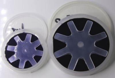
3,58 Oblaten-Magnesium-Oxid-Kristall-Substrat Dichte-MgO-Substrat-/MgO
Preis: by case
MOQ: 10pcs
Lieferzeit: 1-4weeks
Marke: zmkj
Markieren:inp-Oblate, Gap-Oblate
MgO-Substrate, 10X10mm MgO-Oblate, Halbleiterwafer, Magnesiumoxid-(MgO)-Kristallsubstrat, Kristalllieferant MgO-OBLATE 5x5mmProdukt-Beschreibung:Magnesiumoxid (MgO) ist für monokristallines Substrat ist weit verbreitet in der Produktion des ferroelectric Dünnfilms ausgezeichnet, Magnetfilm-, optisch... Mehr sehen
➤ Besuch Webseite
Germanium-einzelne Kristalle Inp-Oblaten-Halbleiter-Substrate
Preis: by case
MOQ: 3pcs
Lieferzeit: 1-4weeks
Marke: zmkj
Markieren:inp-Oblatenhalbleitersubstrate, Halbleiter-Germanium inp-Oblaten, Substrate der einzelnen Kristalle des Germaniums
Germanium-einzelne Kristall-GE-Substrate Oblaten 4inch 6inch, kundengebundene optische Linse GEs
Germaniumsubstrate
Anwendung: Germaniumoblate benutzt in der Produktion des Halbleiterbauelements, optisches Gerät des Infrarotstrahls, sinkendes Material der Solarzelle.
Haupteigentums-Ausd... Mehr sehen
➤ Besuch Webseite

Halb isolierende 2 Art blinder InP-Indium-Phosphid-Wafer des Zoll-50mm N
Preis: by case
MOQ: 3pcs
Lieferzeit: 3-4weeks
Marke: zmkj
Markieren:50mm Indium Phosphid-Oblate, Halb isolierende Indium Phosphid-Oblate, n-Art inp-Oblate
InP-Indium Phosphid-Oblate grad 2inch dia50.8mm n-artige blinde Haupt
Halb-isolierende Phosphid InP-Oblate des Indium-4inch für LD-Laserdiode, Halbleiterwafer, Oblate InP-3inch, einzelne Kristall-wafer2inch 3inch 4inch InP-Substrate für LD-Anwendung, Halbleiterwafer, InP-Oblate, einzelne Kristallsc... Mehr sehen
➤ Besuch Webseite
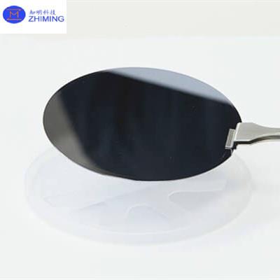
Hohe brechende Oberflächen-GE Germanium-Oblate DSP
Preis: by case
MOQ: 3pcs
Lieferzeit: 1-4weeks
Marke: zmkj
Markieren:DSP-Oberflächengermanium-Oblate, hohe brechende Germanium-Oblate, DSP Oberflächenge-Oblate
Art p-Art 2inch 4inch 6inch N lackierte Germanium-einzelne Kristallscheiben,
Optische Platten der Germanium-einzelnen Kristalle
Fenster GE-Oblate/GE
Germanium (GE) ist das bevorzugte Linsen- und Fenstermaterial für Hochleistungsinfrarotdarstellungssysteme im um Band der Wellenlänge 8-12.... Mehr sehen
➤ Besuch Webseite
GE optische Inp-Oblate, Halbleiterbauelement-Indium-Phosphid-Oblate
Preis: by case
MOQ: 3pcs
Lieferzeit: 1-4weeks
Marke: zmkj
Markieren:GE optische inp-Oblate, Indium-Phosphid-Oblate GEs optische, Halbleiterbauelement inp-Oblate
Germanium-einzelne Kristallscheiben, optische Platten GEs
Germaniumsubstrate
Anwendung: Germaniumoblate benutzt in der Produktion des Halbleiterbauelements, optisches Gerät des Infrarotstrahls, sinkendes Material der Solarzelle.
Haupteigentums-Ausdrücke
Produktionsverfahren... Mehr sehen
➤ Besuch Webseite
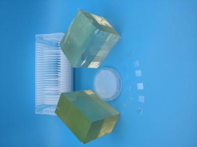
Bogen-Frankreich-Wachstums-Würfel Crystal Mgo Substrates, Magnesium-Oxid-Kristall
Preis: by case
MOQ: 10pcs
Lieferzeit: 1-4weeks
Marke: zmkj
Markieren:Bogen-Frankreich-MgO-Substrate, Berechnen Sie Kristallmgo-Substrate, MgO-Magnesiumoxidkristall
MgO-Substrate, 10X10mm MgO-Oblate, Halbleiterwafer, Kristallsubstrat des Magnesiumoxids (MgO), Kristalllieferant MgO-OBLATE 5x5mmProdukt-Beschreibung:Magnesiumoxid (MgO) ist für monokristallines Substrat ist weitverbreitet in der Produktion des ferroelectric Dünnfilms ausgezeichnet,Magnetfilm-, opti... Mehr sehen
➤ Besuch Webseite

Germanium-einzelne Kristall-Indium-Phosphid-Wafer fertigte optische Linse 4/6 Zoll GEs besonders an
Preis: by case
MOQ: 3pcs
Lieferzeit: 1-4weeks
Marke: zmkj
Markieren:inp-Oblate, Gap-Oblate
Germanium-einzelne Kristall-GE-Substrate Oblaten 4inch 6inch, kundengebundene optische Linse GEs
Germaniumsubstrate
Anwendung: Germaniumoblate benutzt in der Produktion des Halbleiterbauelements, optisches Gerät des Infrarotstrahls, sinkendes Material der Solarzelle.
Haupteigentums-A... Mehr sehen
➤ Besuch Webseite

N / P schreiben Germanium-Oblate, Germanium-Optik-Platten-Durchmesser 0,5 | 150mm
Preis: by case
MOQ: 3pcs
Lieferzeit: 1-4weeks
Marke: zmkj
Markieren:inp-Oblate, MgO-Substrat
Art p-Art 2inch 4inch 6inch N lackierte Germanium-einzelne Kristallscheiben,
Optische Platten der Germanium-einzelnen Kristalle
Fenster GE-Oblate/GE
Germanium (Ge) ist das bevorzugte Linsen- und Fenstermaterial für Hochleistungsinfrarotdarstellungssysteme im um Band der Wellenlänge 8-... Mehr sehen
➤ Besuch Webseite
Primär-/blinde Grad-Indium-Phosphid-Oblaten-Stärke 350um für LD
Preis: by case
MOQ: 3pcs
Lieferzeit: 1-4weeks
Marke: zmkj
Markieren:MgO-Substrat, Gap-Oblate
2inch N-artige P-artige Indium-Phosphid Grad des Primärgrades der Stärke 350um blinde Kristallinp-Substratoblate für LD
Material des einzelnen Kristalles des Indiumphosphids ist eins des meisten wichtigen Halbleitermittels, das Schlüsselrohstoff für Laserdiode des Indiumphosphidsubstrates (LD)... Mehr sehen
➤ Besuch Webseite

Germaniumsubstrat GE Flachfensteroptische Linsen Wärmebildgebung Anwendungen und Infrarotspektroskopie Hohe Härte
Preis: Negotiable
MOQ: Negotiable
Lieferzeit: 2-4 weeks
Marke: ZMSH
Markieren:Anwendungen für die Wärmebildgebung, Infrarotspektroskopie Germaniumsubstrat, Hochhärte-Germaniumsubstrat
Beschreibung des Produkts
Germaniumsubstrat GE Flachfenster Optiklinsen Thermische Bildgebung Anwendungen und Infrarotspektroskopie Hohe Härte
Germaniumfenster (Ge) ist ein chemisch inertes Material mit einem zulässigen Spektrum von 2-12 μm, ein häufig verwendetes Infrarot-Optikmaterial mit hoher H... Mehr sehen
➤ Besuch Webseite
Kupfer-Wärmebecken-Substrat Flachboden-Pin-Typ Hochleistungs-elektronische Vorrichtung Cu≥99,9%
Preis: by case
MOQ: Negotiable
Lieferzeit: 2-4weeks
Marke: ZMSH
Markieren:Cu≥99, 9% Wärmeabwassersubstrat, Hochleistungs-Wärmeabwassersubstrat
Zusammenfassung von cOberwärmeabnehmer-Substrat
Kupfer-Wärmebecken-Substrat Flachboden-Pin-Typ Hochleistungs-elektronische Vorrichtung Cu≥99,9%
Kupfer-Wärmeabwassersubstrat ist ein Wärmeverteilungselement aus reinem Kupfer (Cu≥99,9%) mit hoher Wärmeleitfähigkeit oder aus Kupferlegierung ... Mehr sehen
➤ Besuch Webseite

InAs Indium Arsenid2 Zoll 3 Zoll 4 Zoll Einzelkristall Substrat N/P Typ Halbleiter Wafer Dicke 300-800um
Preis: Negotiable
MOQ: Negotiable
Lieferzeit: 2-4 weeks
Marke: ZMSH
Markieren:4 Zoll Indium-Arsenid-Wafer, 3 Zoll Indium-Arsenid-Wafer, 2 Zoll Indium-Arsenid-Wafer
Beschreibung des Produkts
InAs Indium Arsenid2 Zoll 3 Zoll 4 Zoll Einzelkristall Substrat N/P Typ Halbleiter Wafer Dicke 300-800um
Indium InAs oder Indiumarsenid monolithisch ist ein Halbleiter, der aus Indium und Arsen besteht.Indiumarsenid wird zum Bau von Infrarotdetektoren im Wellenlängenbereic... Mehr sehen
➤ Besuch Webseite
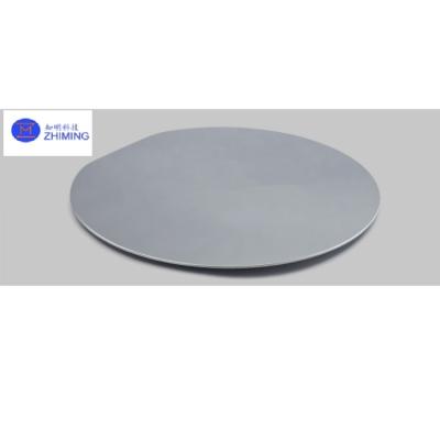
Ge-Germanium Wafer Halbleiter Substrate <111> Konzentrierende Photovoltaik CPV
Preis: Negotiable
MOQ: Negotiable
Lieferzeit: 2-4 weeks
Marke: ZMSH
Markieren:CPV-Germaniumwafer, Germanium-Wafer nach Maß, mit einer Breite von mehr als 20 mm,
Beschreibung des Produkts
Halbleiter-Substrate aus Ge-Germanium-Wafern < 111> zur Konzentration von CPV-Photovoltaik
Germanium hat gute Halbleiter-Eigenschaften. Hochreines Germanium wird mit trivalenten Elementen (z. B. Indium, Gallium, Bor) doppiert, um P-Typ-Germanium-Halbleiter zu erhalte... Mehr sehen
➤ Besuch Webseite
Magnesiumoxid Reinheit 95% MgO Film Substrat 5x5 10x10 20x20 Dicke 0,5 mm 1,0 mm Ausrichtung <001> <110> <111>
Preis: by case
MOQ: 10pcs
Lieferzeit: 1-4weeks
Marke: zmkj
Markieren:5x5 MgO-Foliensubstrat, 20x20 MgO-Filmsubstrat, 10x10 MgO-Filmsubstrat
Magnesiumoxid Reinheit 95% MgO-Filmsubstrat 5x5 10x10 20x20 Dicke 0,5 mm 1,0 mm Ausrichtung <001> <110> <111> Beschreibung des Produkts:
Einzigkristall des Magnesiumoxids (MgO) aus dünnfilmigem Substrat ist ein hochwertiges Substratmaterial mit hervorragenden physikalischen und ... Mehr sehen
➤ Besuch Webseite
InAs Wafer Doped Zn 2 Zoll Indium-Arsenid Wafer Dia 50mm Dicke 500um <100> angepasst
Preis: Negotiable
MOQ: Negotiable
Lieferzeit: 2-4 weeks
Marke: ZMSH
Markieren:Indium-Arsenid-Wafer nach Maß, 2 Zoll Indium-Arsenid-Wafer, 500-um-Indium-Arsenid-Wafer
2 Zoll Indium Arsenid Wafer InAs Epitaxial Wafer für LD Laser Diode, Halbleiter epitaxial Wafer, 3 Zoll InAs-Zn Wafer,InAs Einzelkristallwafer 2 Zoll 3 Zoll 4 Zoll InAs-Zn Substrate für LD Anwendung, Halbleiterwafer, Indium-Arsenid-Laser-Epitaxialwafer Eigenschaften von InAs-Zn-Wafer - InAs-Wafer zu... Mehr sehen
➤ Besuch Webseite
DFB Wafer N-InP Substrat Epiwafer aktive Schicht InGaAlAs/InGaAsP 2 4 6 Zoll für Gassensor
Preis: Negotiable
MOQ: Negotiable
Lieferzeit: 2-4weeks
Marke: ZMSH
Markieren:2 Zoll großer InP-Substrat-Epiwafer, 4 Zoll InP-Substrat-Epiwafer, 6 Zoll InP-Substrat-Epiwafer
DFB Wafer N-InP Substrat Epiwafer aktive Schicht InGaAlAs/InGaAsP 2 4 6 Zoll für Gassensor
DFB Wafer N-InP Substrat Epiwafer Brief
Eine Distributed Feedback (DFB) -Wafer auf einem Indiumphosphat (N-InP) -Substrat des Typ n ist ein kritisches Material, das bei der Herstellung von Hochleistungs-D... Mehr sehen
➤ Besuch Webseite